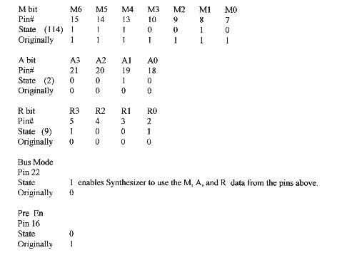
After conversion the Synthesizer Pins are as follows:
Updated April 4, 2000
1152 MHZ Surplus Qualcomm RF/Synthesizer Board Conversion Notes
by N6IZW, K.
Banke 12/1/97 , updated by Ed Munn, W6OYJ
This board measures 5" by 9" and has high harmonic content radiation.
It makes an excellent
source of precision markers through 10368 Mhz. (2304, 3456,
5760, etc). It can be used as
a precision frequency LO source for a 1296 MHz transceiver,
or as a recieving downconverter
for 1296 MHz, or as an up/down converter for 902
MHz. The following description assumes
you view the component side with the 10
Mhz reference oscillator at the lower right
and the power connector at the lower
left. The boards have an identification number on the upper
edge near the left
side. It may be 1DN14ASSY20-6475 or - 30138. See Figure 1.
Low level (-24 dBm) synthesized output is at TP1 . You can replace the connector with an SMA.
U19 is an active upconverter. It has poor performance at 1296 output due to high
LO feedthru -
OK for 902 Mhz upconversion.
U22 is an active downconverter - I.F. output from pin 5 - Works ok at 902 or 1296
input with
144 Mhz IF.
U21 is useful as an amplifier for higher (+7-10 dBm) LO output or upconverter
amp. Ground end of
R62 nearest board edge to turn on U21 & upconverter power.
(See Fig. 4 ). To use board for
1152 LO output only, remove U19
and jumper U19-1 to U19-5 (provides path for LO). Then
jumper across microstrip
filter at top of board near right side. (input to U21). The output
microstrip
filter on right edge near top may be ok to leave in as center freq is about 1.1 GHz.
The preferred method is to install an SMA LO connector at upper right PCB edge,
tied to right
side of C149. For more SMA output, cut the microstrip just to right
of your connection to C149.
The J4 reference connector has the 10 Mhz reference output
For up/down conversion, the J3 IF connector is connected through a filter to a
splitter and then
up and down converters. It also has +15 VDC present. Remove
L56 to remove DC from J3.
Original VCO range is about 750-1000 Mhz. To increase VCO range to 1152 Mhz, use
1000 pF
chip cap to ground at midpoint of PCB loop inductor below Q3. (just below
center screw hole at
top of board, where the Q3 symbol is). See
Fig. 3 for details.
The 10 Mhz reference osc adjustment is accessed by removing the unneeded FL2.
Cut
accessable pins and wiggle until removed with a vise grip. Most of these
osc. have a small
metallic tape covering the adjustment hole.
U2 and U4 , just below the synthesizer chip must be removed as they connect to
the
programming inputs of the synthesizer. A sharp knife can be used to cut the
IC leads close to the
body of the IC and then touching the leads with an iron
will lift them off the board.
The Red LED DS1, above the syn chip is a no lock indicator - It should go off
immediately after
power is applied..
These 1152 boards with a 3216 or 3236 syn chip have an 11-pin power connector
mounted
horizontally along the bottom edge at far left. This is J2. Power connections
are J2-1&2, +15 V @
80 mA, : J2-4&5, +5V @ .42A: J2-3&6, GND.
To change U-1 synthesizer for 1152 Mhz VCO output, you will need to carefully
cut U-1 Pins
#2, 5, 19, and 22 at the pcb pads with a sharp pointed (X-Acto)
knife, and gently lift the IC leads
up away from the pcb. As they are internally
pulled "high" this raises them to the "1" state. See
Figure
2 for locations.
Next you need to ground Pins #7, 9, 10, and 16. See Figure 1 for method.
This board does not have a VCO/2 divider as do the boards we use for conversion
to higher
microwave bands. The synthesizer programming solution for this VCO
to produce 1152.000
output is: N=1152, M=114, A=2, and R=9.
The internal PLL reference frequency is 1 MHz
After conversion the Synthesizer
Pins are as follows:
If you decide to use the PCB as a downconverter for 900 or 1296 Mhz, or an upconverter
for 900
Mhz, you can omit the SMA LO connector installation.
An interactive spreadsheet has been designed to allow you to design for different
VCO frequencies
within the range of this Qualcomm pc board. You can change the
VCo frequency and the PLL frequency
but you must remember they are tied together
by the design rules of the synthesizer, i.e. the VCO must be
an integer multiple
of the PLL frequency. To download this spreadsheet, written in Microsoft Excel format,
click
on SPREADSHEET . The filename is 1152brdc.xls.
Good Luck with your conversion of this board!